Tube PECVD (plasma enhanced chemical vapor deposition) has a wide range of applications in the semiconductor industry. Let’s take a look at the applications of tube PECVD in the semiconductor industry!

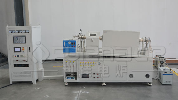
Commonly used tubular PECVD electric furnace (click on the image to view product details)
1. Deposition of thin film materials
PECVD technology can be used for the deposition of various thin film materials in the semiconductor manufacturing process, including but not limited to:
Insulation layer deposition: In semiconductor devices, the insulation layer plays a role in isolation and protection. PECVD technology can accurately deposit high-quality insulation layers, such as silicon nitride (SiN) thin films and silicon dioxide (SiO2) thin films, which have excellent electrical properties and chemical stability.
Passivation layer deposition: Passivation layer is used to protect semiconductor devices from external environmental erosion. PECVD technology can prepare uniform and dense passivation layers, improving the reliability and stability of devices.
Deposition of low-k dielectric materials: With the continuous advancement of semiconductor technology, the demand for low-k dielectric materials is increasing. PECVD technology can prepare dielectric materials with low dielectric constants, which helps to reduce capacitance effects between interconnects and improve device performance.
2. Production of silicon-based optoelectronic devices
PECVD technology also plays a significant role in the production process of silicon-based optoelectronic devices. For example, it can be used to prepare key components such as optical waveguides and gratings, which have important application value in optoelectronic integrated circuits.
3. Solar cells and photovoltaic field
Although the main focus is on the semiconductor field, it is worth mentioning that PECVD technology also has a wide range of applications in the fields of solar cells and photovoltaics. It can be used to prepare key materials such as anti reflective films and transparent conductive films in solar panels.
4. Other applications
In addition, PECVD technology can also be used to prepare key thin film layers in semiconductor memories, as well as to manufacture other functional layers in integrated circuits. These applications fully demonstrate the breadth and importance of PECVD technology in the semiconductor field.
5. Technical advantages
Compared with traditional CVD technology, PECVD technology has advantages such as fast deposition rate, low-temperature operation, strong adaptability, and good film quality. These advantages make PECVD technology have higher application value and competitiveness in the semiconductor field.

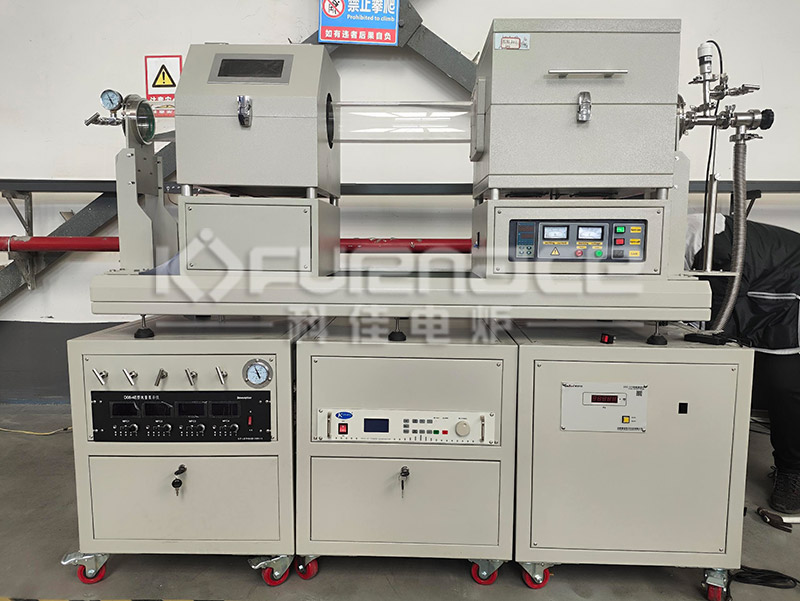
Commonly used PECVD electric furnaces (click on the image to view product details)
In summary, tubular PECVD technology has broad application prospects and important application value in the semiconductor field. With the continuous development of semiconductor technology, PECVD technology will continue to play an important role in semiconductor manufacturing.Click to learn more PECVD devices! Or click on online customer service to learn more about product information!