


Tel Number
181-3719-5600
PECVD (Plasma Enhanced Chemical Vapor Deposition) electric furnace has a wide range of applications in the semiconductor industry. Let’s take a look at the specific applications below!
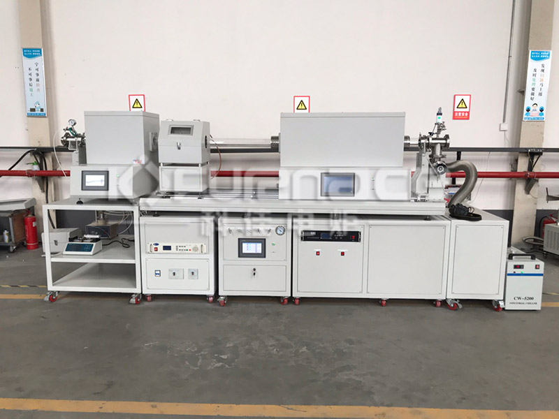
PECVD electric furnace with sliding rail (click on the image to view product details)
1. Integrated circuit manufacturing
Deposition of high-quality thin films: PECVD technology is one of the main techniques for manufacturing integrated circuits in the semiconductor industry. It can deposit high-quality thin films such as silicon dioxide (SiO ₂) and silicon nitride (Si ∝ N ₄) on the substrate surface by precisely controlling process parameters. These films are used to isolate multiple conductive layers and capacitors, and are an important part of integrated circuit manufacturing.
Improving process efficiency: Compared with traditional chemical vapor deposition (CVD), PECVD can deposit at lower temperatures, which not only reduces energy consumption but also protects temperature sensitive substrates, while providing better control accuracy and product quality.
2. Manufacturing of solar cells
Deposition of anti reflective films: PECVD is a key deposition technology for manufacturing solar cells and photovoltaic modules. It can uniformly deposit thin films, such as silicon nitride (SiNx) anti reflective films, on wide surface areas such as solar panels or optical glass. This type of film can fully absorb sunlight, reduce reflection, and protect solar cells from contamination through its passivation effect, thereby improving the photoelectric conversion efficiency of solar cells.
Optimizing battery performance: The generated silicon nitride film contains a large amount of hydrogen, which can effectively passivate dislocations and surface dangling bonds in silicon, improve the mobility of charge carriers in silicon wafers, and thus enhance the overall performance of solar cells.
3. Preparation of optical coatings
Production of coatings with specific optical properties: PECVD technology is also widely used to produce coatings with specific optical properties, such as anti reflective coatings, anti reflective coatings, etc. These coatings can be used for optical products such as sunglasses, colored optical devices, and photometers to improve the optical performance and service life of the products. In the semiconductor industry, these coatings may be used to protect or enhance the optical properties of semiconductor components.
4. Preparation of Nanofilm
Providing high-performance nanofilms: PECVD polymerized nanofilms have the advantages of uniform film thickness, high temperature resistance, wear resistance, and high purity. In the semiconductor industry, these nanofilms can be used to produce internal circuit boards and other components, providing protective functions such as corrosion and moisture resistance, and improving product stability and reliability.
5. Electronic protection
Protecting key components: PECVD polymerized nano films have electronic protection properties and can be used for the protection of semiconductor devices. For example, in key components such as the central control system, boost charging system, and BMS system of new energy vehicles, PECVD nanofilm can improve the stability and safety of the system.
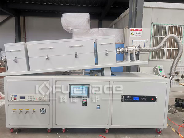
Commonly used PECVD furnaces (click on the image to view product details)
So, the application of PECVD electric furnace in the semiconductor industry is extensive and important, which not only improves the quality and performance of products, but also benefits the progress of semiconductor manufacturing technology. With the continuous development of technology, the application prospects of PECVD electric furnaces in the semiconductor industry will be even broader.Click to learn more PECVD devices! Or click on online customer service to learn more about product information!
Contact Information
E-mail: