


Tel Number
181-3719-5600
CVD furnace (chemical vapor deposition furnace) has a wide range of applications in the semiconductor industry, mainly reflected in the following aspects:
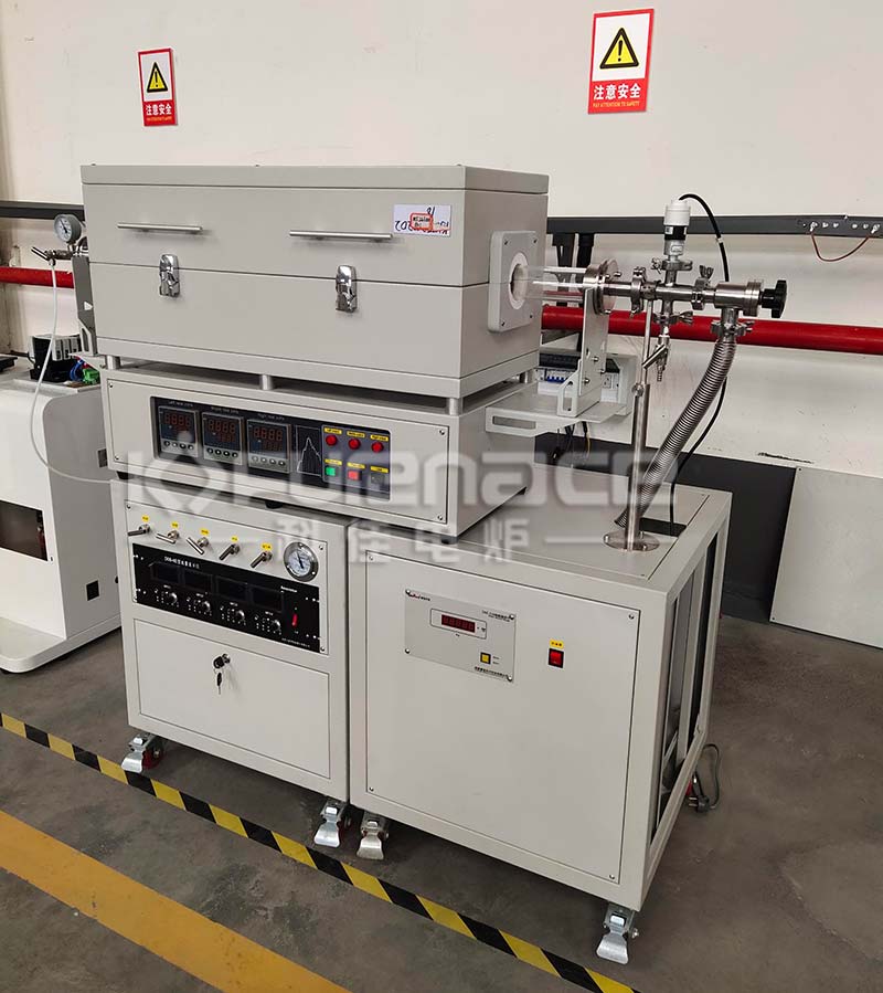
Common CVD furnaces (click on the image to view product details)
1. Material deposition
Insulation layer deposition: CVD furnaces are used to deposit insulation layers such as silicon dioxide (SiO ₂) and silicon nitride (Si ∝ N ₄), which serve as electrical insulation, protection, and passivation in semiconductor devices.
Metal layer deposition: deposition of metal layers such as tungsten (W), titanium (Ti), titanium nitride (TiN), and aluminum (Al), which are mainly used for interconnection and contact hole filling.
Doping layer deposition: such as the deposition of phosphosilicate glass (PSG) and borosilicate glass (BSG), used for local doping and surface passivation to improve the performance of semiconductor devices.
Epitaxial growth: CVD furnaces are also used for epitaxial growth of single crystal silicon or other semiconductor materials (such as silicon carbide and gallium nitride), forming high-quality single crystal layers on the wafer surface, which is important for improving the integration and performance of devices.
High k material deposition: deposition of high k dielectric materials such as hafnium oxide (HfO ₂) and zirconium oxide (ZrO ₂), which are used as MOSFET gate dielectrics to reduce leakage current and improve device performance.
Barrier layer deposition: deposition of titanium nitride (TiN) and tantalum nitride (TaN) as diffusion barriers for copper interconnects, preventing metal diffusion and protecting device integrity.
2. Special material growth
Carbon nanotube and graphene growth: CVD furnaces can be used to grow carbon nanotube and graphene materials, which have wide applications in electronic devices and sensors, such as improving the conductivity, thermal conductivity, and mechanical strength of devices.
Optical and optoelectronic materials: CVD furnaces can also be used to prepare materials for optical and optoelectronic devices, such as gallium nitride (GaN) and other III-V compound semiconductors, which have great applications in fields such as LEDs and lasers.
3. Device manufacturing
Photovoltaic cells: CVD furnaces are used to manufacture thin-film solar cells, such as silicon thin films and compound semiconductor thin films (such as CdTe and CIGS), which have high photoelectric conversion efficiency and are an important component of the renewable energy field.
Micro Electro Mechanical Systems (MEMS): CVD furnaces are also used in MEMS manufacturing, such as depositing materials such as polycrystalline silicon and silicon oxide, for manufacturing micro mechanical structures and sensors.
Gas sensors: By depositing sensitive thin films through CVD, high-sensitivity metal oxide semiconductor gas sensors can be manufactured for use in environmental monitoring and industrial control fields.
4. Other applications
Packaging protective layer: CVD furnace is also used to deposit protective layers to improve packaging reliability and durability, protecting semiconductor devices from external environmental influences.
Through silicon via (TSV): CVD
Furnaces play an important role in the manufacturing of three-dimensional integrated circuits (3D ICs) by depositing high-quality insulation layers and metal filling materials, creating through silicon vias, and achieving three-dimensional interconnection.
5. The application of CVD furnaces in the semiconductor industry has multiple advantages, including:
High purity and high quality: CVD process can deposit high-purity and low defect thin films, ensuring device performance and reliability.
Uniformity and controllability: By precisely controlling the flow rate and reaction conditions of gas-phase reactants, the thickness and composition uniformity of the film can be achieved.
Compatibility and Diversity: CVD technology is suitable for a variety of materials and substrates, and is widely used in different semiconductor manufacturing steps.
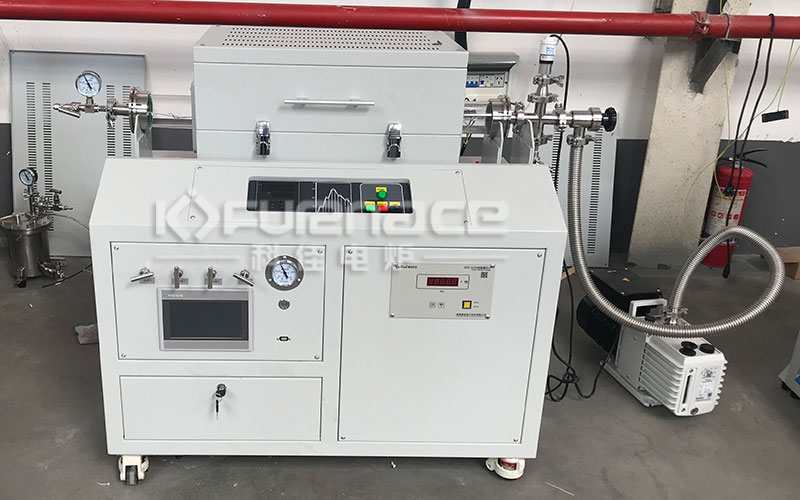
Touchscreen version of 1200 ℃ CVD furnace (click on the image to view product details)
In summary, CVD furnaces play an important role in the semiconductor industry, and their wide range of applications and various advantages enable continuous progress and innovation in semiconductor devices.Click to learn more CVD devices! Or click on online customer service to learn more about product information!
Contact Information
E-mail: