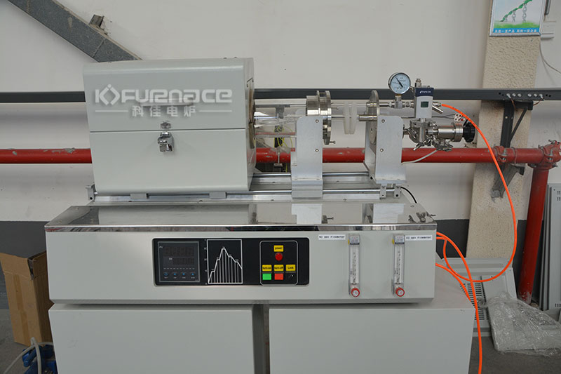
The semiconductor RTP (Rapid Thermal Processing) rapid annealing furnace has great advantages in semiconductor manufacturing and material research. Let’s take a detailed look below!
1. Efficiency
Rapid heating and cooling: The RTP rapid annealing furnace uses high-power heating elements (such as halogen infrared lamps), which can heat the material to the predetermined temperature in a very short time, with a heating rate of up to 100 ℃/s or even higher. At the same time, after annealing is completed, it can quickly cool down, and the entire annealing process can be completed within seconds to minutes, greatly improving production efficiency.
Short process cycle: Compared with traditional furnace tube annealing process, RTP rapid annealing furnace greatly shortens the annealing cycle, reduces production time, and is conducive to reducing production costs.
2. Precise temperature control
High precision temperature control: The RTP rapid annealing furnace is equipped with a high-precision temperature control system that uses PID closed-loop control to monitor and correct the chamber temperature in real time, ensuring the accuracy of temperature control. Under the condition of temperature uniformity ≥ 500 ℃, an accuracy of ≤± 1% can be achieved, ensuring good temperature reproducibility and uniformity.
Multi temperature zone control: Some high-end RTP rapid annealing furnaces have multiple temperature control zones, which can achieve precise temperature control for different zones and meet the needs of complex processes.
3. Optimize material properties
Repairing lattice defects: The high-temperature rapid annealing process of RTP rapid annealing furnace can repair lattice defects generated during ion implantation and other processes, improve the orderliness of crystals, and thus enhance the electronic conductivity of semiconductor materials.
Activating impurities and improving conductivity: Through rapid annealing, the diffusion of impurities in crystalline silicon can be promoted, the concentration and distribution of impurities can be controlled, and the conductivity performance after ion implantation process can be optimized.
Stress relief: High temperature annealing helps alleviate internal stress in semiconductor devices, reduce the formation of crystal defects, and improve material stability and reliability.

Commonly used RTP fast annealing furnace (click on the image to view product details)
4. Flexibility and Scalability
Multi specification processing: RTP rapid annealing furnace is suitable for silicon wafers of various sizes, such as 4 inches, 6 inches, 8 inches, as well as second-generation and third-generation compound materials, such as indium phosphide, gallium arsenide, silicon carbide, gallium nitride, etc.
Gas atmosphere control: RTP rapid annealing furnaces are usually equipped with gas control systems, which can introduce different gas atmospheres (such as argon, nitrogen, oxygen, etc.) according to process requirements to regulate the gas composition inside the chamber and meet the annealing needs of different materials. Some devices can be expanded to 6 sets of process gases, with high flexibility.
Dual cavity or multi cavity design: Some RTP rapid annealing furnaces adopt dual cavity or multi cavity design, which improves production efficiency and reduces process switching time.
5. Safety and reliability
Multiple safety protections: The RTP rapid annealing furnace adopts multiple safety measures such as furnace door safety temperature opening protection, temperature controller opening permission protection, and equipment emergency stop safety protection to comprehensively ensure the safety of instrument use.
Stable process performance: Through precise temperature control and optimized process parameters, RTP rapid annealing furnace can provide a stable and reliable annealing process, ensuring consistency and stability between product batches.
6. Wide range of application areas
RTP rapid annealing furnace has a wide range of applications in semiconductor manufacturing, including:
Ion implantation annealing: repairing ion implantation damage and improving crystal structure.
Growth of oxides and nitrides: Promote the growth of oxides and nitrides, optimize material properties.
Annealing of silicide alloys: forming stable silicide alloys and improving contact performance.
Ohmic contact rapid alloy: By rapid annealing, low contact resistance is formed between the metal electrode and the semiconductor device, improving device performance.
MEMS process: used for annealing treatment of microelectromechanical system (MEMS) devices to optimize device performance.
Compound semiconductor process: annealing treatment for LED chips, optical communication chips, RF chips, power semiconductor chips, etc.
Overall, the semiconductor RTP rapid annealing furnace plays an important role in semiconductor manufacturing and material research due to its high efficiency, precise temperature control, optimized material properties, flexibility and scalability, safety and reliability, and wide range of application fields.Click to learn more tube furnaces! Or click on online customer service to learn more about product information!