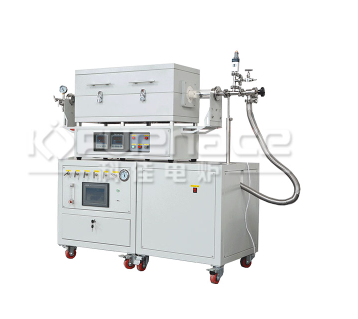
Silicon dioxide deposition CVD electric furnace (i.e. chemical vapor deposition electric furnace) is commonly used in the field of material preparation, especially in semiconductor and microelectronics manufacturing. Let’s take a detailed look at the silicon dioxide deposition CVD electric furnace below!

CVD electric furnace commonly used for silicon dioxide deposition (click on the image to view product details)
1. Working principle
The working principle of CVD electric furnace is mainly based on thermal energy transfer and chemical reactions. Under high temperature conditions, one or more reaction gases sent into the reaction chamber are activated to undergo a chemical reaction, resulting in the formation of solid deposits. These sediments continuously accumulate on the substrate surface, ultimately forming the required thin film or coating.
2. Sedimentary process
Gas transportation: Transport reaction gases such as silicon source gas (such as silane) and oxidants (such as oxygen or nitrogen oxides) to the reaction chamber of the CVD electric furnace.
Gas activation: Under high temperature and possible plasma excitation, the reaction gas is activated and its chemical activity is enhanced.
Chemical reaction: The activated reaction gas undergoes a chemical reaction on the surface of the substrate material, producing silicon dioxide.
Thin film deposition: The generated silicon dioxide continuously accumulates on the substrate to form the desired thin film.
3. Characteristics of deposited thin films
High purity: CVD technology can deposit high-purity silicon dioxide thin films, ensuring device performance and reliability.
Uniformity: By precisely controlling the flow rate and reaction conditions of the reaction gas, the thickness and composition uniformity of the film can be achieved.
Density: The deposited silicon dioxide film has a high density, which helps to improve its physical and electrical properties.
Controllability: By adjusting process parameters such as the composition of reaction gases, flow rate ratio, reaction temperature, etc., the stoichiometric ratio, deposition rate, and performance of deposited thin films can be precisely controlled.
4. Application Fields
Silicon dioxide deposition CVD electric furnace has a wide range of applications in multiple fields:
Semiconductor manufacturing: used for manufacturing transistor gate insulation layers, capacitor dielectric layers, and anti reflection layers for optical devices.
MEMS manufacturing: used for manufacturing passivation layers in micro mechanical structures and sensors.
In the field of optics and optoelectronics: used for preparing optical coatings and sensor components.
5. Equipment features
Efficient heating system: CVD electric furnaces are usually equipped with efficient heating systems that can generate the required high-temperature environment.
Precise control system: equipped with precise temperature control system and gas flow control system to ensure the stability and controllability of the reaction process.
High reliability: Furnace tubes are often made of high-purity materials (such as high-purity quartz tubes), and both ends are sealed with stainless steel high vacuum flanges to ensure airtightness and high temperature resistance.

CVD vacuum tube electric furnace (click on the image to view product details)
Overall, silicon dioxide deposition CVD electric furnaces have broad application prospects and numerous advantages in the field of material preparation. By precisely controlling process parameters and reaction conditions, high-performance silicon dioxide thin films can be prepared to meet the needs of various devices and applications.Click to learn more CVD devices! Or click on online customer service to learn more about product information!