


Tel Number
181-3719-5600
CVD (Chemical Vapor Deposition) can indeed process semiconductor materials and has a wide range of applications in the semiconductor field. Let’s take a closer look at the main applications below!
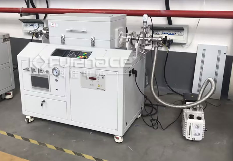
Commonly used CVD electric furnaces (click on the image to view product details)
CVD technology introduces one or more gaseous precursors into a high-temperature reaction chamber. Under appropriate temperature and pressure conditions, these precursors decompose to form the desired solid material, which is then deposited onto a substrate to form a continuous film layer. This technology plays a significant role in semiconductor manufacturing, specifically reflected in the following aspects:
Thin film deposition: CVD technology can be used to deposit various insulation layers, metal layers, and doping layers, such as silicon dioxide (SiO ₂), silicon nitride (Si ∝ N ₄), tungsten (W), titanium (Ti), aluminum (Al), etc. These thin films play a role in electrical insulation, protection, and passivation in semiconductor devices.
Epitaxial growth: CVD is also used for epitaxial growth of single crystal silicon or other semiconductor materials (such as silicon carbide and gallium nitride), forming high-quality single crystal layers on the wafer surface, which is important for improving the performance of semiconductor devices.
Special material deposition: CVD technology can also deposit high-k dielectric materials (such as hafnium oxide HfO ₂ and zirconium oxide ZrO ₂) as MOSFET gate dielectrics to reduce leakage current and improve device performance. In addition, it can also deposit barrier layers (such as titanium nitride TiN and tantalum nitride TaN) to prevent metal diffusion.
Preparation of nanomaterials and special materials: CVD technology can also prepare nanomaterials such as nanoparticles, nanowires, carbon nanotubes, and graphene, which have wide applications in electronic devices and sensors.
Photovoltaic and LED manufacturing: In the photovoltaic field, CVD is used to manufacture thin-film solar cells (such as silicon thin films and compound semiconductor thin films CdTe, CIGS) to improve photoelectric conversion efficiency. In LED and laser manufacturing, CVD is used to deposit gallium nitride (GaN) and other III-V compound semiconductors.
Micro Electro Mechanical Systems (MEMS) and Gas Sensors: CVD technology is also used for material deposition in MEMS manufacturing, as well as for sensitive thin film deposition in metal oxide semiconductor gas sensors, achieving high-sensitivity detection.
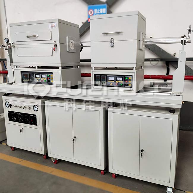
Customized dual body CVD electric furnace (click on the image to view product details)
So, CVD technology has important applications in semiconductor material processing, and its high purity, high quality, uniformity, and controllability have made it widely used in semiconductor manufacturing.Click to learn more CVD devices! Or click on online customer service to learn more about product information!
Contact Information
E-mail: